


Key Insights
The global CdZnTe (CZT) wafer market is experiencing robust expansion, projected to reach an estimated market size of approximately $750 million by 2025, with a remarkable Compound Annual Growth Rate (CAGR) of 12% anticipated through 2033. This significant growth is primarily fueled by the burgeoning demand in the medical sector, particularly for CZT's superior X-ray and gamma-ray detection capabilities essential for advanced imaging devices like SPECT and PET scanners, as well as in security applications for radiation detection. The industrial segment also contributes to this upward trajectory, leveraging CZT in non-destructive testing and industrial inspection equipment. Innovations in detector technology and the increasing adoption of high-performance semiconductor materials are acting as key drivers, pushing the market to new heights.
-Wafer.png)
CdZnTe (CZT) Wafer Market Size (In Million)

However, the market is not without its challenges. The high manufacturing costs associated with CZT wafer production, coupled with the intricate fabrication processes and the need for specialized equipment, present a significant restraint. Furthermore, the availability of alternative detector materials, while not always matching CZT's performance, can pose a competitive threat in certain cost-sensitive applications. The market segmentation reveals a strong preference for larger wafer sizes, with 6” size wafers expected to dominate due to their ability to accommodate more detectors and reduce overall system costs. Geographically, the Asia Pacific region, led by China and India, is emerging as a significant growth hub due to rapid industrialization and increasing healthcare investments, closely followed by North America and Europe, which are established centers for advanced technology development and adoption.
-Wafer.png)
CdZnTe (CZT) Wafer Company Market Share
CdZnTe (CZT) Wafer Market: Comprehensive Analysis & Future Outlook (2019-2033)
This in-depth report provides a panoramic view of the Cadmium Zinc Telluride (CdZnTe) wafer market, encompassing its intricate dynamics, growth trajectory, regional dominance, product landscape, and future potential. Covering the historical period from 2019 to 2024, with a base year of 2025 and an extensive forecast period extending to 2033, this analysis leverages detailed market intelligence to equip industry stakeholders with actionable insights. We delve into parent and child market structures, offering unparalleled clarity on market segmentation and growth drivers. All values are presented in million units for precise financial understanding.
CdZnTe (CZT) Wafer Market Dynamics & Structure
The CdZnTe (CZT) wafer market exhibits a moderately concentrated structure, with a few key players dominating production capabilities, contributing to significant technological innovation drivers. These drivers are primarily centered around enhancing crystal quality, increasing wafer size, and improving detection efficiency for various applications. Regulatory frameworks, particularly those related to material sourcing and environmental compliance, play a crucial role in shaping market entry and operational strategies. Competitive product substitutes, while present in niche areas, have not yet matched the superior radiation detection performance of CZT for critical applications. End-user demographics are increasingly sophisticated, demanding higher purity, larger wafer sizes, and customized specifications. Mergers and acquisitions (M&A) are anticipated to play a role in consolidating market share and expanding technological portfolios. Barriers to innovation are largely tied to the complex manufacturing processes, requiring specialized expertise and significant capital investment.
- Market Concentration: Moderately concentrated with leading players.
- Technological Innovation Drivers: Improved crystal growth, larger wafer diameters, enhanced detection efficiency.
- Regulatory Frameworks: Focus on material sourcing, environmental compliance, and safety standards.
- Competitive Product Substitutes: Limited efficacy in high-performance radiation detection applications.
- End-User Demographics: Demanding high purity, large wafer sizes, and custom specifications.
- M&A Trends: Potential for consolidation and portfolio expansion.
- Innovation Barriers: Complex manufacturing, high capital investment, specialized expertise.
CdZnTe (CZT) Wafer Growth Trends & Insights
The global CdZnTe (CZT) wafer market is poised for robust expansion, driven by escalating demand in its core application segments. The market size is projected to witness a significant CAGR of approximately 12.5% from 2025 to 2033, reaching an estimated value of $550 million by 2033. This growth is fueled by increasing adoption rates in advanced medical imaging, homeland security, and high-energy physics research. Technological disruptions, such as advancements in detector fabrication and signal processing, are enhancing the performance and accessibility of CZT-based devices, leading to a broader spectrum of applications. Consumer behavior shifts are also contributing, with a growing preference for non-destructive testing methods in industrial sectors and a heightened awareness of the benefits of early disease detection in healthcare. The penetration of CZT wafers is expected to accelerate as manufacturing costs decline and performance advantages become more pronounced, making them a critical component in next-generation sensing technologies.
Dominant Regions, Countries, or Segments in CdZnTe (CZT) Wafer
North America currently holds a dominant position in the CdZnTe (CZT) wafer market, driven by its substantial investments in medical research and development, particularly in diagnostic imaging and radiation therapy. The region's strong governmental support for scientific advancement and homeland security initiatives further bolsters demand for high-performance CZT detectors. The United States, as the primary market within North America, benefits from a robust ecosystem of research institutions, detector manufacturers, and end-users. Economically, strong disposable incomes and an aging population in the US are driving demand for advanced medical technologies, where CZT plays a pivotal role in improving diagnostic accuracy and patient outcomes.
Application Segment Dominance:
- Medical: This segment is the primary growth engine for CZT wafers, driven by their exceptional X-ray and gamma-ray detection capabilities, crucial for:
- SPECT and PET Scanners: Enabling higher resolution and faster imaging.
- Handheld Radiation Detectors: Enhancing portability and immediate threat assessment.
- Radiation Therapy Planning: Improving accuracy and reducing off-target exposure.
- Portable Medical Imaging Devices: Facilitating point-of-care diagnostics.
- Market Share: Estimated to command over 60% of the total CZT wafer market by 2033.
- Growth Potential: Continual innovation in detector technology for oncology and cardiology.
Type Segment Dominance:
- 4” Size: While 3” wafers remain a staple, the demand for 4” CZT wafers is rapidly increasing due to their ability to accommodate larger detector arrays, leading to improved imaging performance and reduced system costs.
- Advantages: Enhanced spatial resolution, higher detection efficiency.
- Applications: Increasingly adopted in advanced medical imaging systems and industrial non-destructive testing.
- Market Share: Projected to account for approximately 45% of the market by 2033.
- Growth Potential: Driven by the need for more compact yet powerful imaging solutions.
Industrial Developments:
- Advancements in Crystal Growth Techniques: Innovations in Bridgman and Travelling Heater Method (THM) are yielding higher quality, larger volume CZT crystals, paving the way for bigger wafer diameters.
- Improved Wafer Processing and Characterization: Enhanced polishing and surface treatment techniques are crucial for achieving the stringent purity and uniformity requirements of detector manufacturers.
- Integration with Advanced Readout Electronics: Miniaturization and increased processing power of accompanying electronics are unlocking new functionalities and performance levels for CZT detectors.
CdZnTe (CZT) Wafer Product Landscape
The CdZnTe (CZT) wafer product landscape is characterized by continuous innovation focused on enhancing material purity, increasing crystal size, and optimizing wafer uniformity. Manufacturers are developing advanced growth techniques to produce larger diameter wafers (e.g., 4” and 6” sizes) with minimal defects, thereby improving the performance and cost-effectiveness of radiation detectors. Unique selling propositions lie in CZT's excellent room-temperature operation, high atomic number, and superior energy resolution compared to traditional semiconductor detectors. Technological advancements are enabling its use in portable and miniaturized detector systems, expanding its application spectrum across medical diagnostics, industrial inspection, and scientific research.
Key Drivers, Barriers & Challenges in CdZnTe (CZT) Wafer
Key Drivers:
- Technological Advancements: Superior X-ray and gamma-ray detection capabilities, enabling room-temperature operation and high energy resolution.
- Growing Demand in Healthcare: Increasing use in medical imaging (SPECT, PET), radiation therapy, and portable diagnostic devices for early disease detection and precise treatment.
- Homeland Security Applications: Critical for radiation detection in security screening, border control, and emergency response scenarios.
- Industrial Non-Destructive Testing: Facilitates accurate inspection of materials and structures without damage.
- Scientific Research: Essential component in high-energy physics experiments and astronomical observations.
Key Barriers & Challenges:
- High Manufacturing Costs: Complex crystal growth and wafer fabrication processes contribute to higher production expenses compared to some alternative technologies.
- Material Purity and Defect Control: Achieving and maintaining extremely high material purity and minimizing crystal defects remain ongoing challenges.
- Wafer Size Limitations and Uniformity: Scaling up wafer production to larger diameters while maintaining uniform crystal properties is technically demanding.
- Supply Chain Volatility: Dependence on specific raw materials and specialized manufacturing equipment can lead to supply chain disruptions.
- Regulatory Hurdles: Compliance with stringent regulations in medical and industrial sectors can impact time-to-market.
Emerging Opportunities in CdZnTe (CZT) Wafer
Emerging opportunities in the CdZnTe (CZT) wafer market lie in the development of even larger diameter wafers, pushing the boundaries of detector size and efficiency. Untapped markets include advanced industrial automation for real-time quality control and the burgeoning field of portable, point-of-care medical diagnostics. Evolving consumer preferences for less invasive medical procedures and more sophisticated homeland security tools will further drive demand. Innovations in hybrid detector designs, combining CZT with other semiconductor technologies, also present significant growth potential, offering unique performance characteristics for specialized applications.
Growth Accelerators in the CdZnTe (CZT) Wafer Industry
Long-term growth in the CdZnTe (CZT) wafer industry will be significantly accelerated by breakthroughs in crystal growth techniques that enable larger, higher-quality wafers at reduced costs. Strategic partnerships between wafer manufacturers and detector developers are crucial for co-optimizing materials and designs for specific end-user applications. Furthermore, aggressive market expansion strategies into developing economies with a growing healthcare infrastructure and increasing security concerns will unlock new avenues for growth. The continuous improvement in the performance metrics of CZT detectors, such as quantum efficiency and spectral resolution, will also act as a major catalyst, solidifying its position in demanding applications.
Key Players Shaping the CdZnTe (CZT) Wafer Market
- XIAMEN POWERWAY
- Wafer Technology Ltd
- Hangzhou Shalom Electro-optics Technology
Notable Milestones in CdZnTe (CZT) Wafer Sector
- 2019: Significant improvements in Bridgman crystal growth techniques leading to larger, more uniform CdZnTe ingots.
- 2020: Increased adoption of 4-inch CZT wafers in next-generation SPECT/PET scanner prototypes.
- 2021: Development of advanced wafer processing techniques reducing surface defects and improving detector yield.
- 2022: Enhanced material purity achieved, leading to improved energy resolution in CZT detectors.
- 2023: Increased demand for CZT wafers in portable radiation detection systems for industrial and security applications.
- 2024: Research advancements in CZT detector efficiency for low-energy X-ray applications.
In-Depth CdZnTe (CZT) Wafer Market Outlook
The CdZnTe (CZT) wafer market is projected to experience sustained and significant growth, driven by its indispensable role in critical applications. Growth accelerators such as continued technological advancements in crystal growth, leading to cost reductions and performance enhancements, will be paramount. Strategic alliances between material suppliers and detector manufacturers will foster innovation and streamline product development cycles. The expansion of CZT wafer adoption into emerging markets, particularly in healthcare and security sectors within developing nations, presents substantial untapped potential. The future market outlook is characterized by increasing demand for higher purity, larger diameter wafers, and tailored solutions to meet the evolving needs of sophisticated end-user industries.
CdZnTe (CZT) Wafer Segmentation
-
1. Application
- 1.1. Medical
- 1.2. Industrial
- 1.3. Other
-
2. Types
- 2.1. 3” Size
- 2.2. 4” Size
- 2.3. 6” Size
- 2.4. Other
CdZnTe (CZT) Wafer Segmentation By Geography
-
1. North America
- 1.1. United States
- 1.2. Canada
- 1.3. Mexico
-
2. South America
- 2.1. Brazil
- 2.2. Argentina
- 2.3. Rest of South America
-
3. Europe
- 3.1. United Kingdom
- 3.2. Germany
- 3.3. France
- 3.4. Italy
- 3.5. Spain
- 3.6. Russia
- 3.7. Benelux
- 3.8. Nordics
- 3.9. Rest of Europe
-
4. Middle East & Africa
- 4.1. Turkey
- 4.2. Israel
- 4.3. GCC
- 4.4. North Africa
- 4.5. South Africa
- 4.6. Rest of Middle East & Africa
-
5. Asia Pacific
- 5.1. China
- 5.2. India
- 5.3. Japan
- 5.4. South Korea
- 5.5. ASEAN
- 5.6. Oceania
- 5.7. Rest of Asia Pacific
-Wafer.png)
CdZnTe (CZT) Wafer Regional Market Share
Geographic Coverage of CdZnTe (CZT) Wafer
CdZnTe (CZT) Wafer REPORT HIGHLIGHTS
| Aspects | Details |
|---|---|
| Study Period | 2020-2034 |
| Base Year | 2025 |
| Estimated Year | 2026 |
| Forecast Period | 2026-2034 |
| Historical Period | 2020-2025 |
| Growth Rate | CAGR of 11.7% from 2020-2034 |
| Segmentation |
|
Table of Contents
- 1. Introduction
- 1.1. Research Scope
- 1.2. Market Segmentation
- 1.3. Research Objective
- 1.4. Definitions and Assumptions
- 2. Executive Summary
- 2.1. Market Snapshot
- 3. Market Dynamics
- 3.1. Market Drivers
- 3.2. Market Restrains
- 3.3. Market Trends
- 3.4. Market Opportunities
- 4. Market Factor Analysis
- 4.1. Porters Five Forces
- 4.1.1. Bargaining Power of Suppliers
- 4.1.2. Bargaining Power of Buyers
- 4.1.3. Threat of New Entrants
- 4.1.4. Threat of Substitutes
- 4.1.5. Competitive Rivalry
- 4.2. PESTEL analysis
- 4.3. BCG Analysis
- 4.3.1. Stars (High Growth, High Market Share)
- 4.3.2. Cash Cows (Low Growth, High Market Share)
- 4.3.3. Question Mark (High Growth, Low Market Share)
- 4.3.4. Dogs (Low Growth, Low Market Share)
- 4.4. Ansoff Matrix Analysis
- 4.5. Supply Chain Analysis
- 4.6. Regulatory Landscape
- 4.7. Current Market Potential and Opportunity Assessment (TAM–SAM–SOM Framework)
- 4.8. NRP Analyst Note
- 4.1. Porters Five Forces
- 5. Market Analysis, Insights and Forecast 2021-2033
- 5.1. Market Analysis, Insights and Forecast - by Application
- 5.1.1. Medical
- 5.1.2. Industrial
- 5.1.3. Other
- 5.2. Market Analysis, Insights and Forecast - by Types
- 5.2.1. 3” Size
- 5.2.2. 4” Size
- 5.2.3. 6” Size
- 5.2.4. Other
- 5.3. Market Analysis, Insights and Forecast - by Region
- 5.3.1. North America
- 5.3.2. South America
- 5.3.3. Europe
- 5.3.4. Middle East & Africa
- 5.3.5. Asia Pacific
- 5.1. Market Analysis, Insights and Forecast - by Application
- 6. Global CdZnTe (CZT) Wafer Analysis, Insights and Forecast, 2021-2033
- 6.1. Market Analysis, Insights and Forecast - by Application
- 6.1.1. Medical
- 6.1.2. Industrial
- 6.1.3. Other
- 6.2. Market Analysis, Insights and Forecast - by Types
- 6.2.1. 3” Size
- 6.2.2. 4” Size
- 6.2.3. 6” Size
- 6.2.4. Other
- 6.1. Market Analysis, Insights and Forecast - by Application
- 7. North America CdZnTe (CZT) Wafer Analysis, Insights and Forecast, 2020-2032
- 7.1. Market Analysis, Insights and Forecast - by Application
- 7.1.1. Medical
- 7.1.2. Industrial
- 7.1.3. Other
- 7.2. Market Analysis, Insights and Forecast - by Types
- 7.2.1. 3” Size
- 7.2.2. 4” Size
- 7.2.3. 6” Size
- 7.2.4. Other
- 7.1. Market Analysis, Insights and Forecast - by Application
- 8. South America CdZnTe (CZT) Wafer Analysis, Insights and Forecast, 2020-2032
- 8.1. Market Analysis, Insights and Forecast - by Application
- 8.1.1. Medical
- 8.1.2. Industrial
- 8.1.3. Other
- 8.2. Market Analysis, Insights and Forecast - by Types
- 8.2.1. 3” Size
- 8.2.2. 4” Size
- 8.2.3. 6” Size
- 8.2.4. Other
- 8.1. Market Analysis, Insights and Forecast - by Application
- 9. Europe CdZnTe (CZT) Wafer Analysis, Insights and Forecast, 2020-2032
- 9.1. Market Analysis, Insights and Forecast - by Application
- 9.1.1. Medical
- 9.1.2. Industrial
- 9.1.3. Other
- 9.2. Market Analysis, Insights and Forecast - by Types
- 9.2.1. 3” Size
- 9.2.2. 4” Size
- 9.2.3. 6” Size
- 9.2.4. Other
- 9.1. Market Analysis, Insights and Forecast - by Application
- 10. Middle East & Africa CdZnTe (CZT) Wafer Analysis, Insights and Forecast, 2020-2032
- 10.1. Market Analysis, Insights and Forecast - by Application
- 10.1.1. Medical
- 10.1.2. Industrial
- 10.1.3. Other
- 10.2. Market Analysis, Insights and Forecast - by Types
- 10.2.1. 3” Size
- 10.2.2. 4” Size
- 10.2.3. 6” Size
- 10.2.4. Other
- 10.1. Market Analysis, Insights and Forecast - by Application
- 11. Asia Pacific CdZnTe (CZT) Wafer Analysis, Insights and Forecast, 2020-2032
- 11.1. Market Analysis, Insights and Forecast - by Application
- 11.1.1. Medical
- 11.1.2. Industrial
- 11.1.3. Other
- 11.2. Market Analysis, Insights and Forecast - by Types
- 11.2.1. 3” Size
- 11.2.2. 4” Size
- 11.2.3. 6” Size
- 11.2.4. Other
- 11.1. Market Analysis, Insights and Forecast - by Application
- 12. Competitive Analysis
- 12.1. Company Profiles
- 12.1.1 XIAMEN POWERWAY
- 12.1.1.1. Company Overview
- 12.1.1.2. Products
- 12.1.1.3. Company Financials
- 12.1.1.4. SWOT Analysis
- 12.1.2 Wafer Technology Ltd
- 12.1.2.1. Company Overview
- 12.1.2.2. Products
- 12.1.2.3. Company Financials
- 12.1.2.4. SWOT Analysis
- 12.1.3 Hangzhou Shalom Electro-optics Technology
- 12.1.3.1. Company Overview
- 12.1.3.2. Products
- 12.1.3.3. Company Financials
- 12.1.3.4. SWOT Analysis
- 12.1.1 XIAMEN POWERWAY
- 12.2. Market Entropy
- 12.2.1 Company's Key Areas Served
- 12.2.2 Recent Developments
- 12.3. Company Market Share Analysis 2025
- 12.3.1 Top 5 Companies Market Share Analysis
- 12.3.2 Top 3 Companies Market Share Analysis
- 12.4. List of Potential Customers
- 13. Research Methodology
List of Figures
- Figure 1: Global CdZnTe (CZT) Wafer Revenue Breakdown (undefined, %) by Region 2025 & 2033
- Figure 2: Global CdZnTe (CZT) Wafer Volume Breakdown (K, %) by Region 2025 & 2033
- Figure 3: North America CdZnTe (CZT) Wafer Revenue (undefined), by Application 2025 & 2033
- Figure 4: North America CdZnTe (CZT) Wafer Volume (K), by Application 2025 & 2033
- Figure 5: North America CdZnTe (CZT) Wafer Revenue Share (%), by Application 2025 & 2033
- Figure 6: North America CdZnTe (CZT) Wafer Volume Share (%), by Application 2025 & 2033
- Figure 7: North America CdZnTe (CZT) Wafer Revenue (undefined), by Types 2025 & 2033
- Figure 8: North America CdZnTe (CZT) Wafer Volume (K), by Types 2025 & 2033
- Figure 9: North America CdZnTe (CZT) Wafer Revenue Share (%), by Types 2025 & 2033
- Figure 10: North America CdZnTe (CZT) Wafer Volume Share (%), by Types 2025 & 2033
- Figure 11: North America CdZnTe (CZT) Wafer Revenue (undefined), by Country 2025 & 2033
- Figure 12: North America CdZnTe (CZT) Wafer Volume (K), by Country 2025 & 2033
- Figure 13: North America CdZnTe (CZT) Wafer Revenue Share (%), by Country 2025 & 2033
- Figure 14: North America CdZnTe (CZT) Wafer Volume Share (%), by Country 2025 & 2033
- Figure 15: South America CdZnTe (CZT) Wafer Revenue (undefined), by Application 2025 & 2033
- Figure 16: South America CdZnTe (CZT) Wafer Volume (K), by Application 2025 & 2033
- Figure 17: South America CdZnTe (CZT) Wafer Revenue Share (%), by Application 2025 & 2033
- Figure 18: South America CdZnTe (CZT) Wafer Volume Share (%), by Application 2025 & 2033
- Figure 19: South America CdZnTe (CZT) Wafer Revenue (undefined), by Types 2025 & 2033
- Figure 20: South America CdZnTe (CZT) Wafer Volume (K), by Types 2025 & 2033
- Figure 21: South America CdZnTe (CZT) Wafer Revenue Share (%), by Types 2025 & 2033
- Figure 22: South America CdZnTe (CZT) Wafer Volume Share (%), by Types 2025 & 2033
- Figure 23: South America CdZnTe (CZT) Wafer Revenue (undefined), by Country 2025 & 2033
- Figure 24: South America CdZnTe (CZT) Wafer Volume (K), by Country 2025 & 2033
- Figure 25: South America CdZnTe (CZT) Wafer Revenue Share (%), by Country 2025 & 2033
- Figure 26: South America CdZnTe (CZT) Wafer Volume Share (%), by Country 2025 & 2033
- Figure 27: Europe CdZnTe (CZT) Wafer Revenue (undefined), by Application 2025 & 2033
- Figure 28: Europe CdZnTe (CZT) Wafer Volume (K), by Application 2025 & 2033
- Figure 29: Europe CdZnTe (CZT) Wafer Revenue Share (%), by Application 2025 & 2033
- Figure 30: Europe CdZnTe (CZT) Wafer Volume Share (%), by Application 2025 & 2033
- Figure 31: Europe CdZnTe (CZT) Wafer Revenue (undefined), by Types 2025 & 2033
- Figure 32: Europe CdZnTe (CZT) Wafer Volume (K), by Types 2025 & 2033
- Figure 33: Europe CdZnTe (CZT) Wafer Revenue Share (%), by Types 2025 & 2033
- Figure 34: Europe CdZnTe (CZT) Wafer Volume Share (%), by Types 2025 & 2033
- Figure 35: Europe CdZnTe (CZT) Wafer Revenue (undefined), by Country 2025 & 2033
- Figure 36: Europe CdZnTe (CZT) Wafer Volume (K), by Country 2025 & 2033
- Figure 37: Europe CdZnTe (CZT) Wafer Revenue Share (%), by Country 2025 & 2033
- Figure 38: Europe CdZnTe (CZT) Wafer Volume Share (%), by Country 2025 & 2033
- Figure 39: Middle East & Africa CdZnTe (CZT) Wafer Revenue (undefined), by Application 2025 & 2033
- Figure 40: Middle East & Africa CdZnTe (CZT) Wafer Volume (K), by Application 2025 & 2033
- Figure 41: Middle East & Africa CdZnTe (CZT) Wafer Revenue Share (%), by Application 2025 & 2033
- Figure 42: Middle East & Africa CdZnTe (CZT) Wafer Volume Share (%), by Application 2025 & 2033
- Figure 43: Middle East & Africa CdZnTe (CZT) Wafer Revenue (undefined), by Types 2025 & 2033
- Figure 44: Middle East & Africa CdZnTe (CZT) Wafer Volume (K), by Types 2025 & 2033
- Figure 45: Middle East & Africa CdZnTe (CZT) Wafer Revenue Share (%), by Types 2025 & 2033
- Figure 46: Middle East & Africa CdZnTe (CZT) Wafer Volume Share (%), by Types 2025 & 2033
- Figure 47: Middle East & Africa CdZnTe (CZT) Wafer Revenue (undefined), by Country 2025 & 2033
- Figure 48: Middle East & Africa CdZnTe (CZT) Wafer Volume (K), by Country 2025 & 2033
- Figure 49: Middle East & Africa CdZnTe (CZT) Wafer Revenue Share (%), by Country 2025 & 2033
- Figure 50: Middle East & Africa CdZnTe (CZT) Wafer Volume Share (%), by Country 2025 & 2033
- Figure 51: Asia Pacific CdZnTe (CZT) Wafer Revenue (undefined), by Application 2025 & 2033
- Figure 52: Asia Pacific CdZnTe (CZT) Wafer Volume (K), by Application 2025 & 2033
- Figure 53: Asia Pacific CdZnTe (CZT) Wafer Revenue Share (%), by Application 2025 & 2033
- Figure 54: Asia Pacific CdZnTe (CZT) Wafer Volume Share (%), by Application 2025 & 2033
- Figure 55: Asia Pacific CdZnTe (CZT) Wafer Revenue (undefined), by Types 2025 & 2033
- Figure 56: Asia Pacific CdZnTe (CZT) Wafer Volume (K), by Types 2025 & 2033
- Figure 57: Asia Pacific CdZnTe (CZT) Wafer Revenue Share (%), by Types 2025 & 2033
- Figure 58: Asia Pacific CdZnTe (CZT) Wafer Volume Share (%), by Types 2025 & 2033
- Figure 59: Asia Pacific CdZnTe (CZT) Wafer Revenue (undefined), by Country 2025 & 2033
- Figure 60: Asia Pacific CdZnTe (CZT) Wafer Volume (K), by Country 2025 & 2033
- Figure 61: Asia Pacific CdZnTe (CZT) Wafer Revenue Share (%), by Country 2025 & 2033
- Figure 62: Asia Pacific CdZnTe (CZT) Wafer Volume Share (%), by Country 2025 & 2033
List of Tables
- Table 1: Global CdZnTe (CZT) Wafer Revenue undefined Forecast, by Application 2020 & 2033
- Table 2: Global CdZnTe (CZT) Wafer Volume K Forecast, by Application 2020 & 2033
- Table 3: Global CdZnTe (CZT) Wafer Revenue undefined Forecast, by Types 2020 & 2033
- Table 4: Global CdZnTe (CZT) Wafer Volume K Forecast, by Types 2020 & 2033
- Table 5: Global CdZnTe (CZT) Wafer Revenue undefined Forecast, by Region 2020 & 2033
- Table 6: Global CdZnTe (CZT) Wafer Volume K Forecast, by Region 2020 & 2033
- Table 7: Global CdZnTe (CZT) Wafer Revenue undefined Forecast, by Application 2020 & 2033
- Table 8: Global CdZnTe (CZT) Wafer Volume K Forecast, by Application 2020 & 2033
- Table 9: Global CdZnTe (CZT) Wafer Revenue undefined Forecast, by Types 2020 & 2033
- Table 10: Global CdZnTe (CZT) Wafer Volume K Forecast, by Types 2020 & 2033
- Table 11: Global CdZnTe (CZT) Wafer Revenue undefined Forecast, by Country 2020 & 2033
- Table 12: Global CdZnTe (CZT) Wafer Volume K Forecast, by Country 2020 & 2033
- Table 13: United States CdZnTe (CZT) Wafer Revenue (undefined) Forecast, by Application 2020 & 2033
- Table 14: United States CdZnTe (CZT) Wafer Volume (K) Forecast, by Application 2020 & 2033
- Table 15: Canada CdZnTe (CZT) Wafer Revenue (undefined) Forecast, by Application 2020 & 2033
- Table 16: Canada CdZnTe (CZT) Wafer Volume (K) Forecast, by Application 2020 & 2033
- Table 17: Mexico CdZnTe (CZT) Wafer Revenue (undefined) Forecast, by Application 2020 & 2033
- Table 18: Mexico CdZnTe (CZT) Wafer Volume (K) Forecast, by Application 2020 & 2033
- Table 19: Global CdZnTe (CZT) Wafer Revenue undefined Forecast, by Application 2020 & 2033
- Table 20: Global CdZnTe (CZT) Wafer Volume K Forecast, by Application 2020 & 2033
- Table 21: Global CdZnTe (CZT) Wafer Revenue undefined Forecast, by Types 2020 & 2033
- Table 22: Global CdZnTe (CZT) Wafer Volume K Forecast, by Types 2020 & 2033
- Table 23: Global CdZnTe (CZT) Wafer Revenue undefined Forecast, by Country 2020 & 2033
- Table 24: Global CdZnTe (CZT) Wafer Volume K Forecast, by Country 2020 & 2033
- Table 25: Brazil CdZnTe (CZT) Wafer Revenue (undefined) Forecast, by Application 2020 & 2033
- Table 26: Brazil CdZnTe (CZT) Wafer Volume (K) Forecast, by Application 2020 & 2033
- Table 27: Argentina CdZnTe (CZT) Wafer Revenue (undefined) Forecast, by Application 2020 & 2033
- Table 28: Argentina CdZnTe (CZT) Wafer Volume (K) Forecast, by Application 2020 & 2033
- Table 29: Rest of South America CdZnTe (CZT) Wafer Revenue (undefined) Forecast, by Application 2020 & 2033
- Table 30: Rest of South America CdZnTe (CZT) Wafer Volume (K) Forecast, by Application 2020 & 2033
- Table 31: Global CdZnTe (CZT) Wafer Revenue undefined Forecast, by Application 2020 & 2033
- Table 32: Global CdZnTe (CZT) Wafer Volume K Forecast, by Application 2020 & 2033
- Table 33: Global CdZnTe (CZT) Wafer Revenue undefined Forecast, by Types 2020 & 2033
- Table 34: Global CdZnTe (CZT) Wafer Volume K Forecast, by Types 2020 & 2033
- Table 35: Global CdZnTe (CZT) Wafer Revenue undefined Forecast, by Country 2020 & 2033
- Table 36: Global CdZnTe (CZT) Wafer Volume K Forecast, by Country 2020 & 2033
- Table 37: United Kingdom CdZnTe (CZT) Wafer Revenue (undefined) Forecast, by Application 2020 & 2033
- Table 38: United Kingdom CdZnTe (CZT) Wafer Volume (K) Forecast, by Application 2020 & 2033
- Table 39: Germany CdZnTe (CZT) Wafer Revenue (undefined) Forecast, by Application 2020 & 2033
- Table 40: Germany CdZnTe (CZT) Wafer Volume (K) Forecast, by Application 2020 & 2033
- Table 41: France CdZnTe (CZT) Wafer Revenue (undefined) Forecast, by Application 2020 & 2033
- Table 42: France CdZnTe (CZT) Wafer Volume (K) Forecast, by Application 2020 & 2033
- Table 43: Italy CdZnTe (CZT) Wafer Revenue (undefined) Forecast, by Application 2020 & 2033
- Table 44: Italy CdZnTe (CZT) Wafer Volume (K) Forecast, by Application 2020 & 2033
- Table 45: Spain CdZnTe (CZT) Wafer Revenue (undefined) Forecast, by Application 2020 & 2033
- Table 46: Spain CdZnTe (CZT) Wafer Volume (K) Forecast, by Application 2020 & 2033
- Table 47: Russia CdZnTe (CZT) Wafer Revenue (undefined) Forecast, by Application 2020 & 2033
- Table 48: Russia CdZnTe (CZT) Wafer Volume (K) Forecast, by Application 2020 & 2033
- Table 49: Benelux CdZnTe (CZT) Wafer Revenue (undefined) Forecast, by Application 2020 & 2033
- Table 50: Benelux CdZnTe (CZT) Wafer Volume (K) Forecast, by Application 2020 & 2033
- Table 51: Nordics CdZnTe (CZT) Wafer Revenue (undefined) Forecast, by Application 2020 & 2033
- Table 52: Nordics CdZnTe (CZT) Wafer Volume (K) Forecast, by Application 2020 & 2033
- Table 53: Rest of Europe CdZnTe (CZT) Wafer Revenue (undefined) Forecast, by Application 2020 & 2033
- Table 54: Rest of Europe CdZnTe (CZT) Wafer Volume (K) Forecast, by Application 2020 & 2033
- Table 55: Global CdZnTe (CZT) Wafer Revenue undefined Forecast, by Application 2020 & 2033
- Table 56: Global CdZnTe (CZT) Wafer Volume K Forecast, by Application 2020 & 2033
- Table 57: Global CdZnTe (CZT) Wafer Revenue undefined Forecast, by Types 2020 & 2033
- Table 58: Global CdZnTe (CZT) Wafer Volume K Forecast, by Types 2020 & 2033
- Table 59: Global CdZnTe (CZT) Wafer Revenue undefined Forecast, by Country 2020 & 2033
- Table 60: Global CdZnTe (CZT) Wafer Volume K Forecast, by Country 2020 & 2033
- Table 61: Turkey CdZnTe (CZT) Wafer Revenue (undefined) Forecast, by Application 2020 & 2033
- Table 62: Turkey CdZnTe (CZT) Wafer Volume (K) Forecast, by Application 2020 & 2033
- Table 63: Israel CdZnTe (CZT) Wafer Revenue (undefined) Forecast, by Application 2020 & 2033
- Table 64: Israel CdZnTe (CZT) Wafer Volume (K) Forecast, by Application 2020 & 2033
- Table 65: GCC CdZnTe (CZT) Wafer Revenue (undefined) Forecast, by Application 2020 & 2033
- Table 66: GCC CdZnTe (CZT) Wafer Volume (K) Forecast, by Application 2020 & 2033
- Table 67: North Africa CdZnTe (CZT) Wafer Revenue (undefined) Forecast, by Application 2020 & 2033
- Table 68: North Africa CdZnTe (CZT) Wafer Volume (K) Forecast, by Application 2020 & 2033
- Table 69: South Africa CdZnTe (CZT) Wafer Revenue (undefined) Forecast, by Application 2020 & 2033
- Table 70: South Africa CdZnTe (CZT) Wafer Volume (K) Forecast, by Application 2020 & 2033
- Table 71: Rest of Middle East & Africa CdZnTe (CZT) Wafer Revenue (undefined) Forecast, by Application 2020 & 2033
- Table 72: Rest of Middle East & Africa CdZnTe (CZT) Wafer Volume (K) Forecast, by Application 2020 & 2033
- Table 73: Global CdZnTe (CZT) Wafer Revenue undefined Forecast, by Application 2020 & 2033
- Table 74: Global CdZnTe (CZT) Wafer Volume K Forecast, by Application 2020 & 2033
- Table 75: Global CdZnTe (CZT) Wafer Revenue undefined Forecast, by Types 2020 & 2033
- Table 76: Global CdZnTe (CZT) Wafer Volume K Forecast, by Types 2020 & 2033
- Table 77: Global CdZnTe (CZT) Wafer Revenue undefined Forecast, by Country 2020 & 2033
- Table 78: Global CdZnTe (CZT) Wafer Volume K Forecast, by Country 2020 & 2033
- Table 79: China CdZnTe (CZT) Wafer Revenue (undefined) Forecast, by Application 2020 & 2033
- Table 80: China CdZnTe (CZT) Wafer Volume (K) Forecast, by Application 2020 & 2033
- Table 81: India CdZnTe (CZT) Wafer Revenue (undefined) Forecast, by Application 2020 & 2033
- Table 82: India CdZnTe (CZT) Wafer Volume (K) Forecast, by Application 2020 & 2033
- Table 83: Japan CdZnTe (CZT) Wafer Revenue (undefined) Forecast, by Application 2020 & 2033
- Table 84: Japan CdZnTe (CZT) Wafer Volume (K) Forecast, by Application 2020 & 2033
- Table 85: South Korea CdZnTe (CZT) Wafer Revenue (undefined) Forecast, by Application 2020 & 2033
- Table 86: South Korea CdZnTe (CZT) Wafer Volume (K) Forecast, by Application 2020 & 2033
- Table 87: ASEAN CdZnTe (CZT) Wafer Revenue (undefined) Forecast, by Application 2020 & 2033
- Table 88: ASEAN CdZnTe (CZT) Wafer Volume (K) Forecast, by Application 2020 & 2033
- Table 89: Oceania CdZnTe (CZT) Wafer Revenue (undefined) Forecast, by Application 2020 & 2033
- Table 90: Oceania CdZnTe (CZT) Wafer Volume (K) Forecast, by Application 2020 & 2033
- Table 91: Rest of Asia Pacific CdZnTe (CZT) Wafer Revenue (undefined) Forecast, by Application 2020 & 2033
- Table 92: Rest of Asia Pacific CdZnTe (CZT) Wafer Volume (K) Forecast, by Application 2020 & 2033
Frequently Asked Questions
1. What is the projected Compound Annual Growth Rate (CAGR) of the CdZnTe (CZT) Wafer?
The projected CAGR is approximately 11.7%.
2. Which companies are prominent players in the CdZnTe (CZT) Wafer?
Key companies in the market include XIAMEN POWERWAY, Wafer Technology Ltd, Hangzhou Shalom Electro-optics Technology.
3. What are the main segments of the CdZnTe (CZT) Wafer?
The market segments include Application, Types.
4. Can you provide details about the market size?
The market size is estimated to be USD XXX N/A as of 2022.
5. What are some drivers contributing to market growth?
N/A
6. What are the notable trends driving market growth?
N/A
7. Are there any restraints impacting market growth?
N/A
8. Can you provide examples of recent developments in the market?
N/A
9. What pricing options are available for accessing the report?
Pricing options include single-user, multi-user, and enterprise licenses priced at USD 3950.00, USD 5925.00, and USD 7900.00 respectively.
10. Is the market size provided in terms of value or volume?
The market size is provided in terms of value, measured in N/A and volume, measured in K.
11. Are there any specific market keywords associated with the report?
Yes, the market keyword associated with the report is "CdZnTe (CZT) Wafer," which aids in identifying and referencing the specific market segment covered.
12. How do I determine which pricing option suits my needs best?
The pricing options vary based on user requirements and access needs. Individual users may opt for single-user licenses, while businesses requiring broader access may choose multi-user or enterprise licenses for cost-effective access to the report.
13. Are there any additional resources or data provided in the CdZnTe (CZT) Wafer report?
While the report offers comprehensive insights, it's advisable to review the specific contents or supplementary materials provided to ascertain if additional resources or data are available.
14. How can I stay updated on further developments or reports in the CdZnTe (CZT) Wafer?
To stay informed about further developments, trends, and reports in the CdZnTe (CZT) Wafer, consider subscribing to industry newsletters, following relevant companies and organizations, or regularly checking reputable industry news sources and publications.
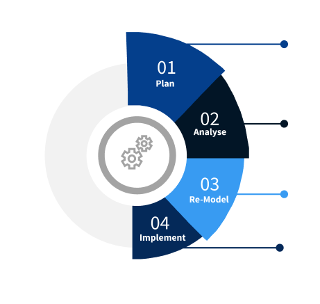
Methodology
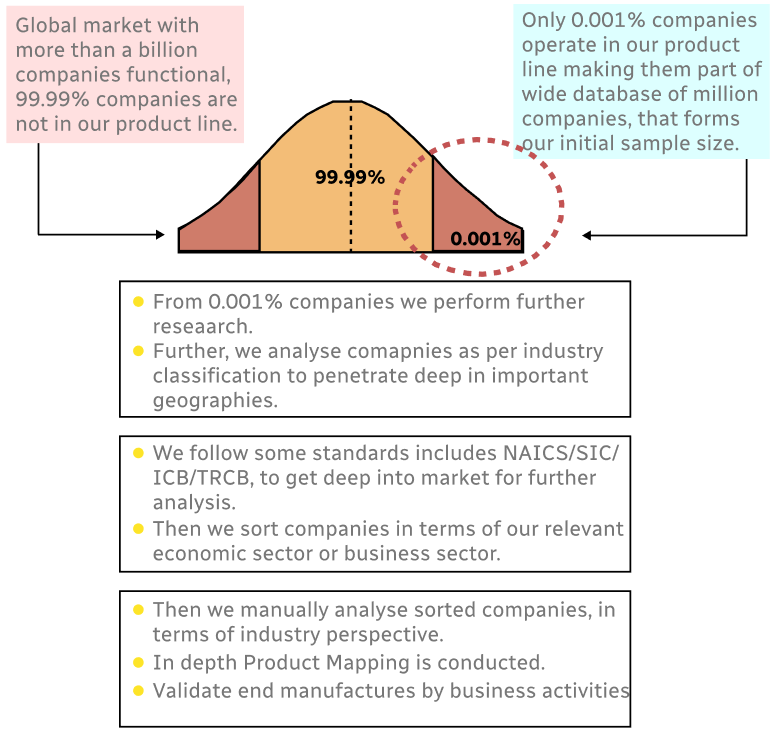
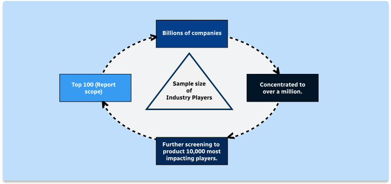
Step 1 - Identification of Relevant Samples Size from Population Database
Step 2 - Approaches for Defining Global Market Size (Value, Volume* & Price*)
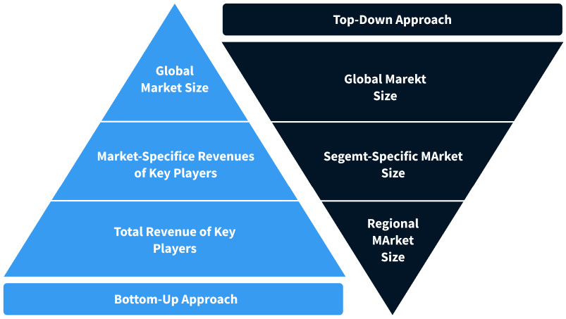
Note*: In applicable scenarios
Step 3 - Data Sources
Primary Research
- Web Analytics
- Survey Reports
- Research Institute
- Latest Research Reports
- Opinion Leaders
Secondary Research
- Annual Reports
- White Paper
- Latest Press Release
- Industry Association
- Paid Database
- Investor Presentations
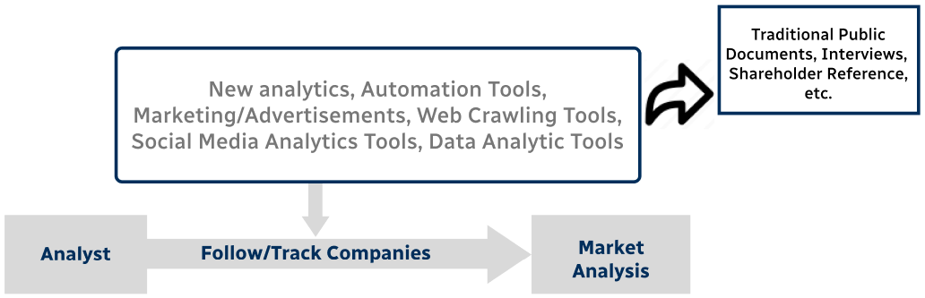
Step 4 - Data Triangulation
Involves using different sources of information in order to increase the validity of a study
These sources are likely to be stakeholders in a program - participants, other researchers, program staff, other community members, and so on.
Then we put all data in single framework & apply various statistical tools to find out the dynamic on the market.
During the analysis stage, feedback from the stakeholder groups would be compared to determine areas of agreement as well as areas of divergence