

Key Insights
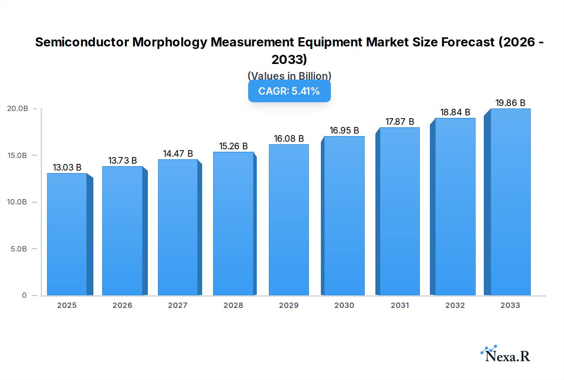
The global Semiconductor Morphology Measurement Equipment market is poised for significant expansion, projected to reach an estimated $13.03 billion in 2025. This robust growth is underpinned by a compound annual growth rate (CAGR) of 5.4%, indicating a sustained upward trajectory through 2033. This burgeoning market is primarily driven by the relentless demand for advanced semiconductor manufacturing processes, which necessitate highly precise and accurate characterization of surface topography and material properties. The increasing complexity of semiconductor devices, coupled with miniaturization trends, places a premium on sophisticated morphology measurement solutions. Furthermore, the critical role of these instruments in semiconductor packaging inspection, ensuring the integrity and performance of integrated circuits, contributes substantially to market demand. The industry is witnessing a dynamic interplay of technological advancements and evolving manufacturing paradigms, all converging to fuel the need for cutting-edge measurement equipment.

Semiconductor Morphology Measurement Equipment Market Size (In Billion)
The market is segmented by application into Semiconductor Manufacturing and Semiconductor Packaging Inspection, with both segments demonstrating strong growth potential. Within types, Optical Profilers and Atomic Force Microscopes (AFMs) are key technologies, each catering to distinct resolution and measurement needs in advanced semiconductor research and production. Leading companies such as KLA, BRUKER, Keyence, and Zygo are at the forefront, investing in R&D to develop next-generation equipment that meets stringent industry requirements. Emerging economies in the Asia Pacific region, particularly China and South Korea, are expected to be major growth centers due to their significant presence in semiconductor fabrication. Conversely, established markets in North America and Europe will continue to be crucial for high-end applications and technological innovation. While the market exhibits strong growth drivers, potential restraints such as the high cost of advanced equipment and the need for skilled operators could influence adoption rates.
Semiconductor Morphology Measurement Equipment Company Market Share
Here is a compelling, SEO-optimized report description for Semiconductor Morphology Measurement Equipment, designed for maximum industry engagement and search engine visibility:
Report Title: Global Semiconductor Morphology Measurement Equipment Market Analysis & Forecast (2019-2033)
Report Description:
Unlock critical insights into the rapidly evolving Global Semiconductor Morphology Measurement Equipment Market. This comprehensive report provides an in-depth analysis of market dynamics, growth trends, and the competitive landscape, essential for stakeholders in semiconductor manufacturing, packaging inspection, and advanced metrology. Delve into the intricate details of leading companies like KLA, BRUKER, Keyence, Zygo, and HORIBA, and understand their strategies shaping the future of semiconductor metrology. With a detailed forecast period from 2025 to 2033, grounded in historical data from 2019-2024 and a base year of 2025, this report is your definitive guide to navigating this high-growth sector.
Semiconductor Morphology Measurement Equipment Market Dynamics & Structure
The semiconductor morphology measurement equipment market is characterized by a moderate to high concentration, dominated by a few key players like KLA and AMETEK, who command significant market share through advanced technological offerings and established customer relationships. However, the increasing number of specialized smaller firms and the growing demand from emerging markets indicate a dynamic competitive environment. Technological innovation is the primary driver, fueled by the relentless pursuit of smaller feature sizes, higher defect detection sensitivity, and faster measurement times in semiconductor fabrication. The ongoing evolution of chip architectures, including 3D NAND and advanced logic nodes, necessitates increasingly sophisticated morphology measurement capabilities. Regulatory frameworks, particularly those promoting domestic semiconductor production and supply chain security (e.g., CHIPS Act in the US, European Chips Act), are indirectly boosting demand by incentivizing investment in advanced manufacturing infrastructure, including metrology tools. Competitive product substitutes are limited, as specialized morphology measurement offers unique, non-replicable insights crucial for process control and yield optimization, though advancements in computational lithography and inline metrology aim to reduce reliance on some offline tools. End-user demographics are shifting towards fabless semiconductor companies and outsourced semiconductor assembly and test (OSAT) providers, who are increasingly investing in in-house metrology solutions to maintain quality and accelerate time-to-market. Mergers and acquisitions (M&A) activity, while not as frequent as in other tech sectors, often involves strategic acquisitions by larger players to gain access to niche technologies or expand their product portfolios, such as acquisitions by KLA or BRUKER to enhance their AFM or optical metrology offerings. The global market size for semiconductor morphology measurement equipment is projected to reach approximately $8.5 billion in 2025 and expand to over $15.2 billion by 2033.
Semiconductor Morphology Measurement Equipment Growth Trends & Insights
The global semiconductor morphology measurement equipment market is poised for robust expansion, driven by the insatiable demand for advanced semiconductors across numerous industries. The market size, estimated at $7.8 billion in the base year of 2025, is projected to witness a compound annual growth rate (CAGR) of approximately 7.2% through the forecast period of 2025-2033. This growth is underpinned by several critical trends. Firstly, the relentless scaling of semiconductor technology, with critical dimensions shrinking to sub-10nm nodes, mandates highly precise and sensitive morphology measurement to ensure defect-free wafer fabrication and packaging. This drives the adoption of advanced techniques such as Atomic Force Microscopy (AFM) and sophisticated Optical Profilers. Secondly, the increasing complexity of semiconductor devices, including the rise of 3D architectures like stacked memory and advanced logic, introduces new challenges in morphology measurement, requiring specialized equipment capable of analyzing intricate 3D structures. The semiconductor manufacturing segment is expected to continue its dominance, accounting for over 75% of the market share in 2025.
Technological disruptions are at the forefront of market evolution. The integration of Artificial Intelligence (AI) and Machine Learning (ML) into metrology systems is a significant trend, enabling faster data analysis, predictive maintenance, and automated defect classification. This enhances the efficiency and accuracy of morphology measurement, reducing the need for manual intervention and accelerating the manufacturing cycle. Furthermore, the development of non-contact measurement techniques is gaining traction, minimizing the risk of sample damage and improving throughput. The shift towards heterogeneous integration and advanced packaging technologies is also creating new avenues for growth. As chips are increasingly integrated in complex 2D and 3D arrangements, the demand for precise morphology measurement at the packaging level, to ensure interconnect integrity and thermal performance, is surging. This is driving the market for specialized inspection tools within the semiconductor packaging inspection segment.
Consumer behavior shifts, particularly the growing demand for high-performance computing, AI-powered devices, 5G infrastructure, and electric vehicles, are indirectly fueling the growth of the semiconductor morphology measurement equipment market. Each of these burgeoning applications requires more advanced and power-efficient semiconductor chips, which in turn necessitates more sophisticated manufacturing and metrology processes. The increased emphasis on supply chain resilience and regional manufacturing capabilities, spurred by geopolitical factors and recent global events, is also leading to significant investments in semiconductor fabrication facilities globally. These new fabs require state-of-the-art metrology equipment to meet stringent quality standards from day one, further accelerating market penetration. The market penetration of advanced morphology measurement techniques, such as AFM for nanoscale surface analysis, is steadily increasing as semiconductor nodes push the boundaries of traditional optical methods. The estimated market size for Semiconductor Morphology Measurement Equipment is $7.8 billion in 2025 and is projected to grow to $15.2 billion by 2033, with a CAGR of 7.2%.
Dominant Regions, Countries, or Segments in Semiconductor Morphology Measurement Equipment
The Application segment of Semiconductor Manufacturing stands as the undisputed leader in driving the growth of the global Semiconductor Morphology Measurement Equipment market. This segment is projected to command a substantial market share of over 75% in 2025, a dominance expected to persist throughout the forecast period. The inherent need for precise control over wafer-level fabrication processes, from lithography and etching to deposition and planarization, directly translates into a high demand for sophisticated morphology measurement tools. As semiconductor manufacturers strive for increasingly smaller feature sizes and more complex device structures, the accuracy and sensitivity of metrology equipment become paramount for ensuring yield and performance. This escalating requirement for defect-free wafer production fuels continuous investment in advanced equipment.
Within the geographical landscape, Asia Pacific is emerging as the dominant region, propelled by its status as the global hub for semiconductor manufacturing and assembly. Countries like Taiwan, South Korea, and China are at the forefront, hosting a significant number of leading foundries and integrated device manufacturers (IDMs). Government initiatives aimed at bolstering domestic semiconductor industries, coupled with substantial private sector investments in advanced fabrication facilities, are creating an unprecedented surge in demand for morphology measurement equipment. For instance, China's ambitious semiconductor self-sufficiency goals are translating into massive investments in new fabs, directly benefiting metrology tool suppliers. Taiwan's established semiconductor ecosystem, home to TSMC, continues to push the boundaries of advanced node manufacturing, requiring the most cutting-edge metrology solutions. South Korea's strong presence in memory manufacturing also drives demand for specialized measurement techniques.
The Type segment of Optical Profiler is another key area contributing significantly to market growth, often serving as the workhorse for critical dimension (CD) uniformity, surface roughness, and step height measurements in semiconductor manufacturing. These tools offer a balance of speed, resolution, and cost-effectiveness, making them indispensable for a wide range of applications. However, the growing complexity of nanoscale features and the need for atomic-level surface characterization are driving the adoption of Atomic Force Microscopes (AFM). Companies like BRUKER are at the forefront of AFM innovation, providing tools essential for advanced research and development and for the most critical process control steps where sub-nanometer precision is required. The symbiotic relationship between optical profilers and AFMs, where each addresses different but complementary measurement needs, ensures continued strong growth across both types. The market for other types of morphology measurement equipment, including stylus profilometers and some specialized electron microscopy techniques, while smaller, caters to specific niche applications and contributes to the overall ecosystem. The market share of the Semiconductor Manufacturing application is expected to be over 75% in 2025, and the Optical Profiler type is anticipated to hold a significant share within the metrology landscape.
Semiconductor Morphology Measurement Equipment Product Landscape
The product landscape for Semiconductor Morphology Measurement Equipment is characterized by relentless innovation focused on enhancing resolution, speed, and versatility. Leading companies like KLA and Keyence are introducing advanced optical profilers with multi-wavelength interferometry and enhanced imaging algorithms for faster, more accurate 3D surface topography analysis. BRUKER is pushing the boundaries of Atomic Force Microscopy (AFM) with higher throughput systems and advanced scanning modes capable of sub-nanometer resolution for detailed surface and material property characterization. 4D Technology and Zygo are known for their innovative interferometric solutions, offering non-contact metrology for complex surfaces and optical components. HORIBA and Mahr continue to offer robust solutions for a range of metrology needs, from surface texture to dimensional measurements. Innovations are increasingly focused on integrating AI and machine learning for automated data analysis and intelligent process feedback, enabling faster yield optimization.
Key Drivers, Barriers & Challenges in Semiconductor Morphology Measurement Equipment
Key Drivers:
- Shrinking Semiconductor Geometries: The continuous drive towards smaller feature sizes in advanced semiconductor nodes necessitates highly precise morphology measurement for defect detection and process control.
- Increasing Device Complexity: The rise of 3D architectures, advanced packaging, and heterogeneous integration requires sophisticated metrology solutions to analyze intricate structures.
- Demand for Higher Yield and Quality: Stringent quality standards across the semiconductor value chain directly translate into a growing need for accurate and reliable morphology measurement.
- Government Initiatives and Investments: Global efforts to boost domestic semiconductor manufacturing are leading to significant investments in new fabs and advanced metrology equipment.
- Growth in Emerging Applications: The demand for high-performance computing, AI, 5G, and automotive electronics drives the need for advanced semiconductor devices and, consequently, advanced metrology.
Barriers & Challenges:
- High Cost of Advanced Equipment: State-of-the-art morphology measurement systems represent a significant capital investment, posing a barrier for smaller companies or those in emerging markets.
- Technological Complexity and Expertise: Operating and interpreting data from advanced metrology equipment requires highly skilled personnel, leading to a talent gap.
- Supply Chain Disruptions: The semiconductor industry's reliance on global supply chains makes it vulnerable to disruptions that can impact equipment availability and lead times.
- Intense Competition and Pricing Pressure: While innovation is high, the market also faces intense competition, leading to pricing pressures on both new and established solutions.
- Integration with Existing Manufacturing Workflows: Seamlessly integrating new metrology tools into existing, often complex, manufacturing execution systems (MES) can be challenging.
Emerging Opportunities in Semiconductor Morphology Measurement Equipment
Emerging opportunities in the Semiconductor Morphology Measurement Equipment market lie in the burgeoning fields of quantum computing, advanced sensor technology, and next-generation displays. The development of novel materials and complex 3D structures for these applications will demand metrology solutions with unprecedented resolution and sensitivity. Furthermore, the growing trend towards Industry 4.0 and smart manufacturing is creating demand for integrated, AI-driven metrology systems that can provide real-time process feedback and predictive analytics. The expansion of semiconductor manufacturing into new geographical regions, driven by national security concerns and supply chain diversification, presents significant untapped markets for equipment suppliers. The increasing adoption of specialized metrology for advanced packaging, including fan-out wafer-level packaging (FOWLP) and chiplet integration, offers substantial growth potential.
Growth Accelerators in the Semiconductor Morphology Measurement Equipment Industry
Several catalysts are accelerating the growth of the Semiconductor Morphology Measurement Equipment industry. Technological breakthroughs in areas like extreme ultraviolet (EUV) lithography and advanced etching processes directly stimulate the need for more precise and sensitive metrology to characterize the resultant nanoscale features. Strategic partnerships between equipment manufacturers and leading semiconductor foundries are crucial for co-developing tailored solutions that address the evolving challenges of next-generation chip manufacturing. Market expansion strategies, including establishing strong service and support networks in high-growth regions like Southeast Asia and India, are vital for capturing new customer bases. Furthermore, the ongoing consolidation and M&A activities by major players aim to broaden product portfolios and expand market reach, consolidating their dominance and driving further innovation through synergistic integration of technologies.
Key Players Shaping the Semiconductor Morphology Measurement Equipment Market
- KLA
- BRUKER
- Keyence
- Zygo
- 4D Technology
- HORIBA
- Mahr
- Sensofar
- Semilab
- CAMTEK
- Park Systems
- Taylor Hobson
- Skyverse Technology
- AMETEK
- Polytec
Notable Milestones in Semiconductor Morphology Measurement Equipment Sector
- 2021: KLA launches a new suite of inspection and metrology solutions for advanced packaging, addressing growing demand for heterogeneous integration.
- 2020: BRUKER expands its Dimension Icon AFM product line with enhanced capabilities for nanoscale imaging and material characterization.
- 2019: Keyence introduces a new generation of optical profilers offering higher speed and resolution for semiconductor wafer inspection.
- 2022: Zygo announces advancements in its Verifire™ interferometers, improving measurement accuracy for critical optical components in semiconductor manufacturing.
- 2023: AMETEK acquires a specialized metrology company, enhancing its portfolio in advanced semiconductor inspection tools.
- Ongoing: Continuous development and integration of AI/ML capabilities into existing product lines by various key players for enhanced data analysis and automation.
In-Depth Semiconductor Morphology Measurement Equipment Market Outlook
The future outlook for the Semiconductor Morphology Measurement Equipment market is exceptionally bright, driven by sustained demand for advanced semiconductors and continuous technological innovation. Growth accelerators like the miniaturization of chip architectures, the rise of AI and 5G, and global investments in semiconductor manufacturing infrastructure will continue to propel market expansion. Strategic opportunities lie in developing metrology solutions for emerging semiconductor materials, quantum computing components, and advanced packaging technologies. The increasing emphasis on smart manufacturing and data-driven process control will favor vendors offering integrated, AI-enabled metrology platforms. The market is set for sustained growth, with significant potential for market leaders to capitalize on innovation and geographical expansion.
Semiconductor Morphology Measurement Equipment Segmentation
-
1. Application
- 1.1. Semiconductor Manufacturing
- 1.2. Semiconductor Packaging Inspection
-
2. Types
- 2.1. Optical Profiler
- 2.2. Atomic Force Microscope
- 2.3. Other
Semiconductor Morphology Measurement Equipment Segmentation By Geography
-
1. North America
- 1.1. United States
- 1.2. Canada
- 1.3. Mexico
-
2. South America
- 2.1. Brazil
- 2.2. Argentina
- 2.3. Rest of South America
-
3. Europe
- 3.1. United Kingdom
- 3.2. Germany
- 3.3. France
- 3.4. Italy
- 3.5. Spain
- 3.6. Russia
- 3.7. Benelux
- 3.8. Nordics
- 3.9. Rest of Europe
-
4. Middle East & Africa
- 4.1. Turkey
- 4.2. Israel
- 4.3. GCC
- 4.4. North Africa
- 4.5. South Africa
- 4.6. Rest of Middle East & Africa
-
5. Asia Pacific
- 5.1. China
- 5.2. India
- 5.3. Japan
- 5.4. South Korea
- 5.5. ASEAN
- 5.6. Oceania
- 5.7. Rest of Asia Pacific
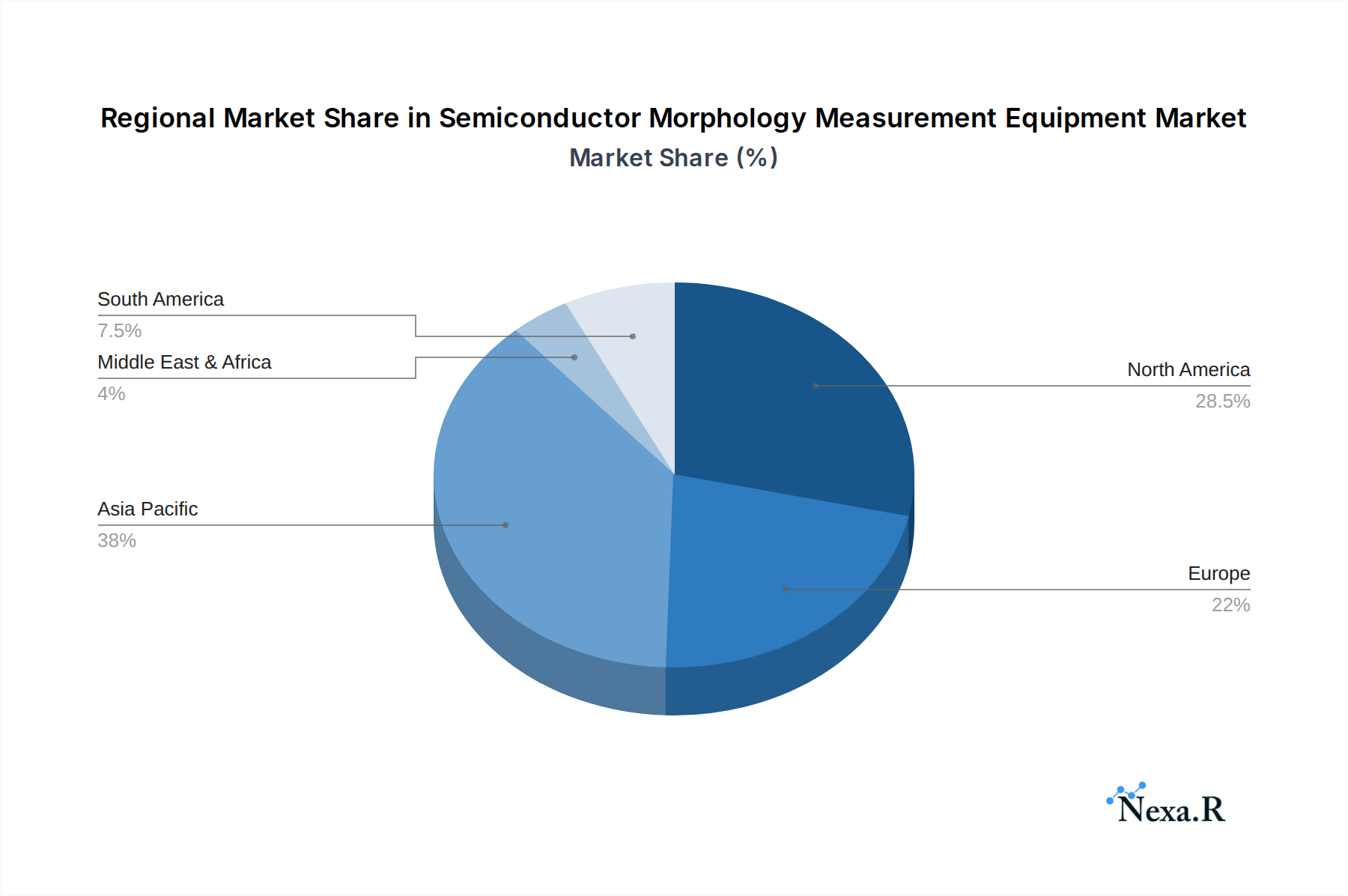
Semiconductor Morphology Measurement Equipment Regional Market Share
Geographic Coverage of Semiconductor Morphology Measurement Equipment
Semiconductor Morphology Measurement Equipment REPORT HIGHLIGHTS
| Aspects | Details |
|---|---|
| Study Period | 2020-2034 |
| Base Year | 2025 |
| Estimated Year | 2026 |
| Forecast Period | 2026-2034 |
| Historical Period | 2020-2025 |
| Growth Rate | CAGR of 5.4% from 2020-2034 |
| Segmentation |
|
Table of Contents
- 1. Introduction
- 1.1. Research Scope
- 1.2. Market Segmentation
- 1.3. Research Methodology
- 1.4. Definitions and Assumptions
- 2. Executive Summary
- 2.1. Introduction
- 3. Market Dynamics
- 3.1. Introduction
- 3.2. Market Drivers
- 3.3. Market Restrains
- 3.4. Market Trends
- 4. Market Factor Analysis
- 4.1. Porters Five Forces
- 4.2. Supply/Value Chain
- 4.3. PESTEL analysis
- 4.4. Market Entropy
- 4.5. Patent/Trademark Analysis
- 5. Global Semiconductor Morphology Measurement Equipment Analysis, Insights and Forecast, 2020-2032
- 5.1. Market Analysis, Insights and Forecast - by Application
- 5.1.1. Semiconductor Manufacturing
- 5.1.2. Semiconductor Packaging Inspection
- 5.2. Market Analysis, Insights and Forecast - by Types
- 5.2.1. Optical Profiler
- 5.2.2. Atomic Force Microscope
- 5.2.3. Other
- 5.3. Market Analysis, Insights and Forecast - by Region
- 5.3.1. North America
- 5.3.2. South America
- 5.3.3. Europe
- 5.3.4. Middle East & Africa
- 5.3.5. Asia Pacific
- 5.1. Market Analysis, Insights and Forecast - by Application
- 6. North America Semiconductor Morphology Measurement Equipment Analysis, Insights and Forecast, 2020-2032
- 6.1. Market Analysis, Insights and Forecast - by Application
- 6.1.1. Semiconductor Manufacturing
- 6.1.2. Semiconductor Packaging Inspection
- 6.2. Market Analysis, Insights and Forecast - by Types
- 6.2.1. Optical Profiler
- 6.2.2. Atomic Force Microscope
- 6.2.3. Other
- 6.1. Market Analysis, Insights and Forecast - by Application
- 7. South America Semiconductor Morphology Measurement Equipment Analysis, Insights and Forecast, 2020-2032
- 7.1. Market Analysis, Insights and Forecast - by Application
- 7.1.1. Semiconductor Manufacturing
- 7.1.2. Semiconductor Packaging Inspection
- 7.2. Market Analysis, Insights and Forecast - by Types
- 7.2.1. Optical Profiler
- 7.2.2. Atomic Force Microscope
- 7.2.3. Other
- 7.1. Market Analysis, Insights and Forecast - by Application
- 8. Europe Semiconductor Morphology Measurement Equipment Analysis, Insights and Forecast, 2020-2032
- 8.1. Market Analysis, Insights and Forecast - by Application
- 8.1.1. Semiconductor Manufacturing
- 8.1.2. Semiconductor Packaging Inspection
- 8.2. Market Analysis, Insights and Forecast - by Types
- 8.2.1. Optical Profiler
- 8.2.2. Atomic Force Microscope
- 8.2.3. Other
- 8.1. Market Analysis, Insights and Forecast - by Application
- 9. Middle East & Africa Semiconductor Morphology Measurement Equipment Analysis, Insights and Forecast, 2020-2032
- 9.1. Market Analysis, Insights and Forecast - by Application
- 9.1.1. Semiconductor Manufacturing
- 9.1.2. Semiconductor Packaging Inspection
- 9.2. Market Analysis, Insights and Forecast - by Types
- 9.2.1. Optical Profiler
- 9.2.2. Atomic Force Microscope
- 9.2.3. Other
- 9.1. Market Analysis, Insights and Forecast - by Application
- 10. Asia Pacific Semiconductor Morphology Measurement Equipment Analysis, Insights and Forecast, 2020-2032
- 10.1. Market Analysis, Insights and Forecast - by Application
- 10.1.1. Semiconductor Manufacturing
- 10.1.2. Semiconductor Packaging Inspection
- 10.2. Market Analysis, Insights and Forecast - by Types
- 10.2.1. Optical Profiler
- 10.2.2. Atomic Force Microscope
- 10.2.3. Other
- 10.1. Market Analysis, Insights and Forecast - by Application
- 11. Competitive Analysis
- 11.1. Global Market Share Analysis 2025
- 11.2. Company Profiles
- 11.2.1 KLA
- 11.2.1.1. Overview
- 11.2.1.2. Products
- 11.2.1.3. SWOT Analysis
- 11.2.1.4. Recent Developments
- 11.2.1.5. Financials (Based on Availability)
- 11.2.2 BRUKER
- 11.2.2.1. Overview
- 11.2.2.2. Products
- 11.2.2.3. SWOT Analysis
- 11.2.2.4. Recent Developments
- 11.2.2.5. Financials (Based on Availability)
- 11.2.3 Keyence
- 11.2.3.1. Overview
- 11.2.3.2. Products
- 11.2.3.3. SWOT Analysis
- 11.2.3.4. Recent Developments
- 11.2.3.5. Financials (Based on Availability)
- 11.2.4 Zygo
- 11.2.4.1. Overview
- 11.2.4.2. Products
- 11.2.4.3. SWOT Analysis
- 11.2.4.4. Recent Developments
- 11.2.4.5. Financials (Based on Availability)
- 11.2.5 4D Technology
- 11.2.5.1. Overview
- 11.2.5.2. Products
- 11.2.5.3. SWOT Analysis
- 11.2.5.4. Recent Developments
- 11.2.5.5. Financials (Based on Availability)
- 11.2.6 HORIBA
- 11.2.6.1. Overview
- 11.2.6.2. Products
- 11.2.6.3. SWOT Analysis
- 11.2.6.4. Recent Developments
- 11.2.6.5. Financials (Based on Availability)
- 11.2.7 Mahr
- 11.2.7.1. Overview
- 11.2.7.2. Products
- 11.2.7.3. SWOT Analysis
- 11.2.7.4. Recent Developments
- 11.2.7.5. Financials (Based on Availability)
- 11.2.8 Sensofar
- 11.2.8.1. Overview
- 11.2.8.2. Products
- 11.2.8.3. SWOT Analysis
- 11.2.8.4. Recent Developments
- 11.2.8.5. Financials (Based on Availability)
- 11.2.9 Semilab
- 11.2.9.1. Overview
- 11.2.9.2. Products
- 11.2.9.3. SWOT Analysis
- 11.2.9.4. Recent Developments
- 11.2.9.5. Financials (Based on Availability)
- 11.2.10 CAMTEK
- 11.2.10.1. Overview
- 11.2.10.2. Products
- 11.2.10.3. SWOT Analysis
- 11.2.10.4. Recent Developments
- 11.2.10.5. Financials (Based on Availability)
- 11.2.11 Park Systems
- 11.2.11.1. Overview
- 11.2.11.2. Products
- 11.2.11.3. SWOT Analysis
- 11.2.11.4. Recent Developments
- 11.2.11.5. Financials (Based on Availability)
- 11.2.12 Taylor Hobson
- 11.2.12.1. Overview
- 11.2.12.2. Products
- 11.2.12.3. SWOT Analysis
- 11.2.12.4. Recent Developments
- 11.2.12.5. Financials (Based on Availability)
- 11.2.13 Skyverse Technology
- 11.2.13.1. Overview
- 11.2.13.2. Products
- 11.2.13.3. SWOT Analysis
- 11.2.13.4. Recent Developments
- 11.2.13.5. Financials (Based on Availability)
- 11.2.14 AMETEK
- 11.2.14.1. Overview
- 11.2.14.2. Products
- 11.2.14.3. SWOT Analysis
- 11.2.14.4. Recent Developments
- 11.2.14.5. Financials (Based on Availability)
- 11.2.15 Polytec
- 11.2.15.1. Overview
- 11.2.15.2. Products
- 11.2.15.3. SWOT Analysis
- 11.2.15.4. Recent Developments
- 11.2.15.5. Financials (Based on Availability)
- 11.2.1 KLA
List of Figures
- Figure 1: Global Semiconductor Morphology Measurement Equipment Revenue Breakdown (billion, %) by Region 2025 & 2033
- Figure 2: Global Semiconductor Morphology Measurement Equipment Volume Breakdown (K, %) by Region 2025 & 2033
- Figure 3: North America Semiconductor Morphology Measurement Equipment Revenue (billion), by Application 2025 & 2033
- Figure 4: North America Semiconductor Morphology Measurement Equipment Volume (K), by Application 2025 & 2033
- Figure 5: North America Semiconductor Morphology Measurement Equipment Revenue Share (%), by Application 2025 & 2033
- Figure 6: North America Semiconductor Morphology Measurement Equipment Volume Share (%), by Application 2025 & 2033
- Figure 7: North America Semiconductor Morphology Measurement Equipment Revenue (billion), by Types 2025 & 2033
- Figure 8: North America Semiconductor Morphology Measurement Equipment Volume (K), by Types 2025 & 2033
- Figure 9: North America Semiconductor Morphology Measurement Equipment Revenue Share (%), by Types 2025 & 2033
- Figure 10: North America Semiconductor Morphology Measurement Equipment Volume Share (%), by Types 2025 & 2033
- Figure 11: North America Semiconductor Morphology Measurement Equipment Revenue (billion), by Country 2025 & 2033
- Figure 12: North America Semiconductor Morphology Measurement Equipment Volume (K), by Country 2025 & 2033
- Figure 13: North America Semiconductor Morphology Measurement Equipment Revenue Share (%), by Country 2025 & 2033
- Figure 14: North America Semiconductor Morphology Measurement Equipment Volume Share (%), by Country 2025 & 2033
- Figure 15: South America Semiconductor Morphology Measurement Equipment Revenue (billion), by Application 2025 & 2033
- Figure 16: South America Semiconductor Morphology Measurement Equipment Volume (K), by Application 2025 & 2033
- Figure 17: South America Semiconductor Morphology Measurement Equipment Revenue Share (%), by Application 2025 & 2033
- Figure 18: South America Semiconductor Morphology Measurement Equipment Volume Share (%), by Application 2025 & 2033
- Figure 19: South America Semiconductor Morphology Measurement Equipment Revenue (billion), by Types 2025 & 2033
- Figure 20: South America Semiconductor Morphology Measurement Equipment Volume (K), by Types 2025 & 2033
- Figure 21: South America Semiconductor Morphology Measurement Equipment Revenue Share (%), by Types 2025 & 2033
- Figure 22: South America Semiconductor Morphology Measurement Equipment Volume Share (%), by Types 2025 & 2033
- Figure 23: South America Semiconductor Morphology Measurement Equipment Revenue (billion), by Country 2025 & 2033
- Figure 24: South America Semiconductor Morphology Measurement Equipment Volume (K), by Country 2025 & 2033
- Figure 25: South America Semiconductor Morphology Measurement Equipment Revenue Share (%), by Country 2025 & 2033
- Figure 26: South America Semiconductor Morphology Measurement Equipment Volume Share (%), by Country 2025 & 2033
- Figure 27: Europe Semiconductor Morphology Measurement Equipment Revenue (billion), by Application 2025 & 2033
- Figure 28: Europe Semiconductor Morphology Measurement Equipment Volume (K), by Application 2025 & 2033
- Figure 29: Europe Semiconductor Morphology Measurement Equipment Revenue Share (%), by Application 2025 & 2033
- Figure 30: Europe Semiconductor Morphology Measurement Equipment Volume Share (%), by Application 2025 & 2033
- Figure 31: Europe Semiconductor Morphology Measurement Equipment Revenue (billion), by Types 2025 & 2033
- Figure 32: Europe Semiconductor Morphology Measurement Equipment Volume (K), by Types 2025 & 2033
- Figure 33: Europe Semiconductor Morphology Measurement Equipment Revenue Share (%), by Types 2025 & 2033
- Figure 34: Europe Semiconductor Morphology Measurement Equipment Volume Share (%), by Types 2025 & 2033
- Figure 35: Europe Semiconductor Morphology Measurement Equipment Revenue (billion), by Country 2025 & 2033
- Figure 36: Europe Semiconductor Morphology Measurement Equipment Volume (K), by Country 2025 & 2033
- Figure 37: Europe Semiconductor Morphology Measurement Equipment Revenue Share (%), by Country 2025 & 2033
- Figure 38: Europe Semiconductor Morphology Measurement Equipment Volume Share (%), by Country 2025 & 2033
- Figure 39: Middle East & Africa Semiconductor Morphology Measurement Equipment Revenue (billion), by Application 2025 & 2033
- Figure 40: Middle East & Africa Semiconductor Morphology Measurement Equipment Volume (K), by Application 2025 & 2033
- Figure 41: Middle East & Africa Semiconductor Morphology Measurement Equipment Revenue Share (%), by Application 2025 & 2033
- Figure 42: Middle East & Africa Semiconductor Morphology Measurement Equipment Volume Share (%), by Application 2025 & 2033
- Figure 43: Middle East & Africa Semiconductor Morphology Measurement Equipment Revenue (billion), by Types 2025 & 2033
- Figure 44: Middle East & Africa Semiconductor Morphology Measurement Equipment Volume (K), by Types 2025 & 2033
- Figure 45: Middle East & Africa Semiconductor Morphology Measurement Equipment Revenue Share (%), by Types 2025 & 2033
- Figure 46: Middle East & Africa Semiconductor Morphology Measurement Equipment Volume Share (%), by Types 2025 & 2033
- Figure 47: Middle East & Africa Semiconductor Morphology Measurement Equipment Revenue (billion), by Country 2025 & 2033
- Figure 48: Middle East & Africa Semiconductor Morphology Measurement Equipment Volume (K), by Country 2025 & 2033
- Figure 49: Middle East & Africa Semiconductor Morphology Measurement Equipment Revenue Share (%), by Country 2025 & 2033
- Figure 50: Middle East & Africa Semiconductor Morphology Measurement Equipment Volume Share (%), by Country 2025 & 2033
- Figure 51: Asia Pacific Semiconductor Morphology Measurement Equipment Revenue (billion), by Application 2025 & 2033
- Figure 52: Asia Pacific Semiconductor Morphology Measurement Equipment Volume (K), by Application 2025 & 2033
- Figure 53: Asia Pacific Semiconductor Morphology Measurement Equipment Revenue Share (%), by Application 2025 & 2033
- Figure 54: Asia Pacific Semiconductor Morphology Measurement Equipment Volume Share (%), by Application 2025 & 2033
- Figure 55: Asia Pacific Semiconductor Morphology Measurement Equipment Revenue (billion), by Types 2025 & 2033
- Figure 56: Asia Pacific Semiconductor Morphology Measurement Equipment Volume (K), by Types 2025 & 2033
- Figure 57: Asia Pacific Semiconductor Morphology Measurement Equipment Revenue Share (%), by Types 2025 & 2033
- Figure 58: Asia Pacific Semiconductor Morphology Measurement Equipment Volume Share (%), by Types 2025 & 2033
- Figure 59: Asia Pacific Semiconductor Morphology Measurement Equipment Revenue (billion), by Country 2025 & 2033
- Figure 60: Asia Pacific Semiconductor Morphology Measurement Equipment Volume (K), by Country 2025 & 2033
- Figure 61: Asia Pacific Semiconductor Morphology Measurement Equipment Revenue Share (%), by Country 2025 & 2033
- Figure 62: Asia Pacific Semiconductor Morphology Measurement Equipment Volume Share (%), by Country 2025 & 2033
List of Tables
- Table 1: Global Semiconductor Morphology Measurement Equipment Revenue billion Forecast, by Application 2020 & 2033
- Table 2: Global Semiconductor Morphology Measurement Equipment Volume K Forecast, by Application 2020 & 2033
- Table 3: Global Semiconductor Morphology Measurement Equipment Revenue billion Forecast, by Types 2020 & 2033
- Table 4: Global Semiconductor Morphology Measurement Equipment Volume K Forecast, by Types 2020 & 2033
- Table 5: Global Semiconductor Morphology Measurement Equipment Revenue billion Forecast, by Region 2020 & 2033
- Table 6: Global Semiconductor Morphology Measurement Equipment Volume K Forecast, by Region 2020 & 2033
- Table 7: Global Semiconductor Morphology Measurement Equipment Revenue billion Forecast, by Application 2020 & 2033
- Table 8: Global Semiconductor Morphology Measurement Equipment Volume K Forecast, by Application 2020 & 2033
- Table 9: Global Semiconductor Morphology Measurement Equipment Revenue billion Forecast, by Types 2020 & 2033
- Table 10: Global Semiconductor Morphology Measurement Equipment Volume K Forecast, by Types 2020 & 2033
- Table 11: Global Semiconductor Morphology Measurement Equipment Revenue billion Forecast, by Country 2020 & 2033
- Table 12: Global Semiconductor Morphology Measurement Equipment Volume K Forecast, by Country 2020 & 2033
- Table 13: United States Semiconductor Morphology Measurement Equipment Revenue (billion) Forecast, by Application 2020 & 2033
- Table 14: United States Semiconductor Morphology Measurement Equipment Volume (K) Forecast, by Application 2020 & 2033
- Table 15: Canada Semiconductor Morphology Measurement Equipment Revenue (billion) Forecast, by Application 2020 & 2033
- Table 16: Canada Semiconductor Morphology Measurement Equipment Volume (K) Forecast, by Application 2020 & 2033
- Table 17: Mexico Semiconductor Morphology Measurement Equipment Revenue (billion) Forecast, by Application 2020 & 2033
- Table 18: Mexico Semiconductor Morphology Measurement Equipment Volume (K) Forecast, by Application 2020 & 2033
- Table 19: Global Semiconductor Morphology Measurement Equipment Revenue billion Forecast, by Application 2020 & 2033
- Table 20: Global Semiconductor Morphology Measurement Equipment Volume K Forecast, by Application 2020 & 2033
- Table 21: Global Semiconductor Morphology Measurement Equipment Revenue billion Forecast, by Types 2020 & 2033
- Table 22: Global Semiconductor Morphology Measurement Equipment Volume K Forecast, by Types 2020 & 2033
- Table 23: Global Semiconductor Morphology Measurement Equipment Revenue billion Forecast, by Country 2020 & 2033
- Table 24: Global Semiconductor Morphology Measurement Equipment Volume K Forecast, by Country 2020 & 2033
- Table 25: Brazil Semiconductor Morphology Measurement Equipment Revenue (billion) Forecast, by Application 2020 & 2033
- Table 26: Brazil Semiconductor Morphology Measurement Equipment Volume (K) Forecast, by Application 2020 & 2033
- Table 27: Argentina Semiconductor Morphology Measurement Equipment Revenue (billion) Forecast, by Application 2020 & 2033
- Table 28: Argentina Semiconductor Morphology Measurement Equipment Volume (K) Forecast, by Application 2020 & 2033
- Table 29: Rest of South America Semiconductor Morphology Measurement Equipment Revenue (billion) Forecast, by Application 2020 & 2033
- Table 30: Rest of South America Semiconductor Morphology Measurement Equipment Volume (K) Forecast, by Application 2020 & 2033
- Table 31: Global Semiconductor Morphology Measurement Equipment Revenue billion Forecast, by Application 2020 & 2033
- Table 32: Global Semiconductor Morphology Measurement Equipment Volume K Forecast, by Application 2020 & 2033
- Table 33: Global Semiconductor Morphology Measurement Equipment Revenue billion Forecast, by Types 2020 & 2033
- Table 34: Global Semiconductor Morphology Measurement Equipment Volume K Forecast, by Types 2020 & 2033
- Table 35: Global Semiconductor Morphology Measurement Equipment Revenue billion Forecast, by Country 2020 & 2033
- Table 36: Global Semiconductor Morphology Measurement Equipment Volume K Forecast, by Country 2020 & 2033
- Table 37: United Kingdom Semiconductor Morphology Measurement Equipment Revenue (billion) Forecast, by Application 2020 & 2033
- Table 38: United Kingdom Semiconductor Morphology Measurement Equipment Volume (K) Forecast, by Application 2020 & 2033
- Table 39: Germany Semiconductor Morphology Measurement Equipment Revenue (billion) Forecast, by Application 2020 & 2033
- Table 40: Germany Semiconductor Morphology Measurement Equipment Volume (K) Forecast, by Application 2020 & 2033
- Table 41: France Semiconductor Morphology Measurement Equipment Revenue (billion) Forecast, by Application 2020 & 2033
- Table 42: France Semiconductor Morphology Measurement Equipment Volume (K) Forecast, by Application 2020 & 2033
- Table 43: Italy Semiconductor Morphology Measurement Equipment Revenue (billion) Forecast, by Application 2020 & 2033
- Table 44: Italy Semiconductor Morphology Measurement Equipment Volume (K) Forecast, by Application 2020 & 2033
- Table 45: Spain Semiconductor Morphology Measurement Equipment Revenue (billion) Forecast, by Application 2020 & 2033
- Table 46: Spain Semiconductor Morphology Measurement Equipment Volume (K) Forecast, by Application 2020 & 2033
- Table 47: Russia Semiconductor Morphology Measurement Equipment Revenue (billion) Forecast, by Application 2020 & 2033
- Table 48: Russia Semiconductor Morphology Measurement Equipment Volume (K) Forecast, by Application 2020 & 2033
- Table 49: Benelux Semiconductor Morphology Measurement Equipment Revenue (billion) Forecast, by Application 2020 & 2033
- Table 50: Benelux Semiconductor Morphology Measurement Equipment Volume (K) Forecast, by Application 2020 & 2033
- Table 51: Nordics Semiconductor Morphology Measurement Equipment Revenue (billion) Forecast, by Application 2020 & 2033
- Table 52: Nordics Semiconductor Morphology Measurement Equipment Volume (K) Forecast, by Application 2020 & 2033
- Table 53: Rest of Europe Semiconductor Morphology Measurement Equipment Revenue (billion) Forecast, by Application 2020 & 2033
- Table 54: Rest of Europe Semiconductor Morphology Measurement Equipment Volume (K) Forecast, by Application 2020 & 2033
- Table 55: Global Semiconductor Morphology Measurement Equipment Revenue billion Forecast, by Application 2020 & 2033
- Table 56: Global Semiconductor Morphology Measurement Equipment Volume K Forecast, by Application 2020 & 2033
- Table 57: Global Semiconductor Morphology Measurement Equipment Revenue billion Forecast, by Types 2020 & 2033
- Table 58: Global Semiconductor Morphology Measurement Equipment Volume K Forecast, by Types 2020 & 2033
- Table 59: Global Semiconductor Morphology Measurement Equipment Revenue billion Forecast, by Country 2020 & 2033
- Table 60: Global Semiconductor Morphology Measurement Equipment Volume K Forecast, by Country 2020 & 2033
- Table 61: Turkey Semiconductor Morphology Measurement Equipment Revenue (billion) Forecast, by Application 2020 & 2033
- Table 62: Turkey Semiconductor Morphology Measurement Equipment Volume (K) Forecast, by Application 2020 & 2033
- Table 63: Israel Semiconductor Morphology Measurement Equipment Revenue (billion) Forecast, by Application 2020 & 2033
- Table 64: Israel Semiconductor Morphology Measurement Equipment Volume (K) Forecast, by Application 2020 & 2033
- Table 65: GCC Semiconductor Morphology Measurement Equipment Revenue (billion) Forecast, by Application 2020 & 2033
- Table 66: GCC Semiconductor Morphology Measurement Equipment Volume (K) Forecast, by Application 2020 & 2033
- Table 67: North Africa Semiconductor Morphology Measurement Equipment Revenue (billion) Forecast, by Application 2020 & 2033
- Table 68: North Africa Semiconductor Morphology Measurement Equipment Volume (K) Forecast, by Application 2020 & 2033
- Table 69: South Africa Semiconductor Morphology Measurement Equipment Revenue (billion) Forecast, by Application 2020 & 2033
- Table 70: South Africa Semiconductor Morphology Measurement Equipment Volume (K) Forecast, by Application 2020 & 2033
- Table 71: Rest of Middle East & Africa Semiconductor Morphology Measurement Equipment Revenue (billion) Forecast, by Application 2020 & 2033
- Table 72: Rest of Middle East & Africa Semiconductor Morphology Measurement Equipment Volume (K) Forecast, by Application 2020 & 2033
- Table 73: Global Semiconductor Morphology Measurement Equipment Revenue billion Forecast, by Application 2020 & 2033
- Table 74: Global Semiconductor Morphology Measurement Equipment Volume K Forecast, by Application 2020 & 2033
- Table 75: Global Semiconductor Morphology Measurement Equipment Revenue billion Forecast, by Types 2020 & 2033
- Table 76: Global Semiconductor Morphology Measurement Equipment Volume K Forecast, by Types 2020 & 2033
- Table 77: Global Semiconductor Morphology Measurement Equipment Revenue billion Forecast, by Country 2020 & 2033
- Table 78: Global Semiconductor Morphology Measurement Equipment Volume K Forecast, by Country 2020 & 2033
- Table 79: China Semiconductor Morphology Measurement Equipment Revenue (billion) Forecast, by Application 2020 & 2033
- Table 80: China Semiconductor Morphology Measurement Equipment Volume (K) Forecast, by Application 2020 & 2033
- Table 81: India Semiconductor Morphology Measurement Equipment Revenue (billion) Forecast, by Application 2020 & 2033
- Table 82: India Semiconductor Morphology Measurement Equipment Volume (K) Forecast, by Application 2020 & 2033
- Table 83: Japan Semiconductor Morphology Measurement Equipment Revenue (billion) Forecast, by Application 2020 & 2033
- Table 84: Japan Semiconductor Morphology Measurement Equipment Volume (K) Forecast, by Application 2020 & 2033
- Table 85: South Korea Semiconductor Morphology Measurement Equipment Revenue (billion) Forecast, by Application 2020 & 2033
- Table 86: South Korea Semiconductor Morphology Measurement Equipment Volume (K) Forecast, by Application 2020 & 2033
- Table 87: ASEAN Semiconductor Morphology Measurement Equipment Revenue (billion) Forecast, by Application 2020 & 2033
- Table 88: ASEAN Semiconductor Morphology Measurement Equipment Volume (K) Forecast, by Application 2020 & 2033
- Table 89: Oceania Semiconductor Morphology Measurement Equipment Revenue (billion) Forecast, by Application 2020 & 2033
- Table 90: Oceania Semiconductor Morphology Measurement Equipment Volume (K) Forecast, by Application 2020 & 2033
- Table 91: Rest of Asia Pacific Semiconductor Morphology Measurement Equipment Revenue (billion) Forecast, by Application 2020 & 2033
- Table 92: Rest of Asia Pacific Semiconductor Morphology Measurement Equipment Volume (K) Forecast, by Application 2020 & 2033
Frequently Asked Questions
1. What is the projected Compound Annual Growth Rate (CAGR) of the Semiconductor Morphology Measurement Equipment?
The projected CAGR is approximately 5.4%.
2. Which companies are prominent players in the Semiconductor Morphology Measurement Equipment?
Key companies in the market include KLA, BRUKER, Keyence, Zygo, 4D Technology, HORIBA, Mahr, Sensofar, Semilab, CAMTEK, Park Systems, Taylor Hobson, Skyverse Technology, AMETEK, Polytec.
3. What are the main segments of the Semiconductor Morphology Measurement Equipment?
The market segments include Application, Types.
4. Can you provide details about the market size?
The market size is estimated to be USD 13.03 billion as of 2022.
5. What are some drivers contributing to market growth?
N/A
6. What are the notable trends driving market growth?
N/A
7. Are there any restraints impacting market growth?
N/A
8. Can you provide examples of recent developments in the market?
N/A
9. What pricing options are available for accessing the report?
Pricing options include single-user, multi-user, and enterprise licenses priced at USD 3950.00, USD 5925.00, and USD 7900.00 respectively.
10. Is the market size provided in terms of value or volume?
The market size is provided in terms of value, measured in billion and volume, measured in K.
11. Are there any specific market keywords associated with the report?
Yes, the market keyword associated with the report is "Semiconductor Morphology Measurement Equipment," which aids in identifying and referencing the specific market segment covered.
12. How do I determine which pricing option suits my needs best?
The pricing options vary based on user requirements and access needs. Individual users may opt for single-user licenses, while businesses requiring broader access may choose multi-user or enterprise licenses for cost-effective access to the report.
13. Are there any additional resources or data provided in the Semiconductor Morphology Measurement Equipment report?
While the report offers comprehensive insights, it's advisable to review the specific contents or supplementary materials provided to ascertain if additional resources or data are available.
14. How can I stay updated on further developments or reports in the Semiconductor Morphology Measurement Equipment?
To stay informed about further developments, trends, and reports in the Semiconductor Morphology Measurement Equipment, consider subscribing to industry newsletters, following relevant companies and organizations, or regularly checking reputable industry news sources and publications.
Methodology
Step 1 - Identification of Relevant Samples Size from Population Database


Step 2 - Approaches for Defining Global Market Size (Value, Volume* & Price*)

Note*: In applicable scenarios
Step 3 - Data Sources
Primary Research
- Web Analytics
- Survey Reports
- Research Institute
- Latest Research Reports
- Opinion Leaders
Secondary Research
- Annual Reports
- White Paper
- Latest Press Release
- Industry Association
- Paid Database
- Investor Presentations

Step 4 - Data Triangulation
Involves using different sources of information in order to increase the validity of a study
These sources are likely to be stakeholders in a program - participants, other researchers, program staff, other community members, and so on.
Then we put all data in single framework & apply various statistical tools to find out the dynamic on the market.
During the analysis stage, feedback from the stakeholder groups would be compared to determine areas of agreement as well as areas of divergence